
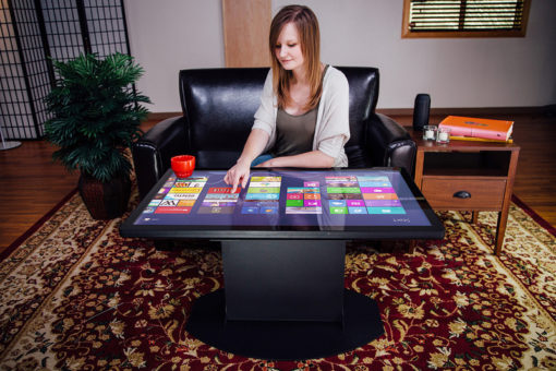
The combination of nanowires and silver has led to the implementation of transparent conductors on which are based the new multitasking 42” touchscreens usable horizontally, precisely as if we were facing a desk.
They are actually silver nanowires, whose characteristics and properties are originating innovative applications, to the extent that we can state we are facing a new technology.
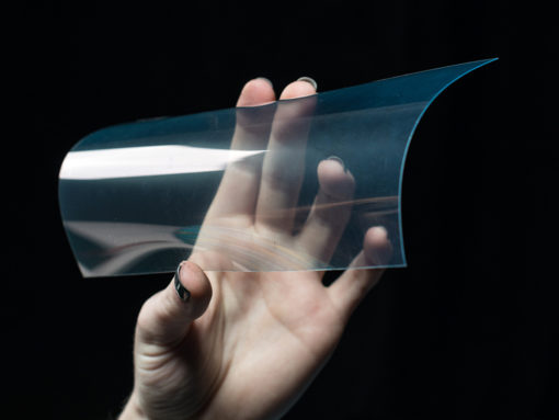
Nanowires, according to an unofficial but commonly shared definition, are nanostructures, whose diameter is in the order of the nanometre, i.e. 10−9 metres. Another more specific definition is based on what is indicated as “aspect-ratio”, meaning with that the length-width ratio, which must be higher than 1000, hence also a characterization of nanowires as unidimensional, or 1D, structures, unlike the usual three-dimensional, bulk or 3D structures, such as for instance standard electric cables. With these sizes, the effects are referable to quantum mechanics, physical theory that describes the behaviour of the material on atomic and sub-atomic scale and they are so important as to lead to the definition of “quantum wire”, electrical conductors where, precisely, quantum effects influence the transport properties of electrons, for instance the electrical conductance. The other protagonist, so to say, of this article is silver that, among all metals, turns out to be the best conductor of electricity in nature, having resistivity or specific electrical resistance, to be meant as opposition to the passage of electrical charges, of just 1.59 x 10⁻⁸ ohm per metre, lower than copper one (1.68 x 10⁻⁸ ohm/m) and the gold one (2.35 x 10⁻⁸ ohm/m). The matching of nanowires and silver has led to the implementation of transparent conductors “silver nanowire-based” that have allowed the production of new highly performing electronic devices, innovative also in terms of use modalities: prime example are the new multi-user 42” touchscreens, usable horizontally, just as if you were sitting in front of a desk, and on the other hand it would be very uncomfortable to operate with a screen of these sizes vertically. Anyway, before reaching this step, some preliminary considerations about the current technologies and the future proposed by silver nanowires.
Displays are everywhere
In daily practice, terms like display, screen or monitor are indifferently used to indicate a flat, more or less subtle surface where can be displayed images, videos or data coming from electronic devices such as PC, TV or smartphones. Therefore, in more academic terms, they are visualization units, with variable sizes, which can range, highly simplifying, from the simpler seven-segment displays, aimed at representing decimal or hexadecimal digits, with precisely seven luminous segments per digit, to CRT screens, nowadays undoubtedly disappeared, up to pixel matrix screens, based on liquid crystal display (LCD technology), without forgetting plasma screens, specific for a certain TV typology. Currently, we can state that the “touch age” has started, with the diffusion of touchscreens, screens sensitive to the touch. An example is constituted by capacitive screens: when a finger, conductor of electricity, touches the screen, it determines a variation of surface capacity that is acquired by a matrix of condensers equipping a panel under the glass surface, with the consequent activation of the interactions wished by the user. Market expectations are oriented towards light, luminous and well-visible touchscreens under whatever light condition, but at same time less and less expensive and increasingly performing in the interaction with the user: from the technological point of view, this is attainable only through the use of highly transparent conductive elements, absolutely invisible to human eye. The drivers concerning displays are essentially the enhancement of the “user experience” and the product differentiation, and this starting from the release on the market of the first iPhone Apple in 2007. The pervasiveness of touchscreens has then increased with the introduction of Windows 8, Microsoft operating system that integrates a touch function. In view of the differentiation and of the user experience increment, several manufacturers have developed “large” screens, also flexible, but the limit for the implementation of a real technological progress within the reach of a broad segment of users, in terms of costs, has remained: the impossibility of replacing the current transparent conductors with others that can combine low costs of the material and of manufacturing processes with flexibility, high electrical conductivity and high optical performances.
The ITO approach
The vast majority of the current touchscreens for PC, smartphones and tablets is based on ITO (Indium Tin Oxide), as transparent conductive material.
The vast majority of the current touchscreens for PC, smartphones and tablets is based on ITO (Indium Tin Oxide), as transparent conductive material, solid solution of indium and tin oxide, one of the most commonly used for the manufacturing of transparent conductive films or sheets, which grants a good compromise between electrical conductivity and optical transparency, defined the latter as the physical property that allows light to cross a material. ITO is a ceramic material that is processed through vacuum deposition at high temperatures, process that determines its very expensive production. Some manufacturers have staked on ITO to develop large screens but this solution is not ideal because, besides being expensive, leads to implement fragile, not subtle and heavy glass substrates, and in the case of flexible screens, which need thin plastic substrates, their electrical and optical performances undergo a notable decay, since the material of the substrate limits the temperature of machining and deposition of ITO, not to mention the possibility of rolling up the screens, made impossible by the material tendency to break. Apart from all that, there is a boost to find an alternative to ITO for the “indium” component, rare material and also geopolitically critical, since it mainly comes from the zinc machining in China and, if until now an efficiency increase in the the machining and recycling of worn-out screens had permitted to maintain a balance between the market offer and demand, in perspective this is no longer possible. Actually, to face the growing demand for touchscreens, it is indispensable to find an alternative conductive and transparent material. And here silver nanowires come into play.
A new technology
Even if giving up indium and tin oxide is still condidered a difficult challenge in some ways, also owing to the huge investments that manufacturers have lavished in the ITO technology, alternatives are not missing and the first is represented by graphene, material that features a monoatomic layer of carbon atoms, having then a thickness equivalent to the sizes of a single atom, whose characteristics include a high electrical conductivity performance, even at a limit of nominal concentration equal to zero of charge carriers, in addition to sturdiness, flexibility and transparency. Manufacturing processes, however, are still complex and several years will go by before it becomes commercially available. A solution might also come from the technology called “Roll-to-roll metal mesh”, anyway once solved the basic problem: to make metal lines so thin as to be substantially invisible when coupled with a display. Finally, and here a reaI new technology emerges, there are silver nanowires: a grid of silver nanowires allows implementing highly conductive layers with excellent transparency and unequalled flexibility. Moreover, not only silver is about 100-time more conductive than the indium-tin oxide, but also the production of nanowires provides for much lower costs than for ITO, and it can take place at low temperatures, with advantages in the electrical conductivity characteristics of flexible plastic substrates, avoiding the degradation caused by the high temperatures needed with ITO. If we highlight more in detail the performances of silver nanowires as transparent conductors compared to the indium-tin oxide, it is worth considering two parameters: light transmission and sheet resistance. The first is measured as light percentage that crosses the transparent conductor, and a high value can increment efficiency and duration of the battery of mobile devices, since the backlight of the device must not be excessively luminous. Concerning the sheet resistance, applicable to bi-dimensional entities like a film or a sheet having uniform thickness (measured in ohms but exclusively used for the sheet resistance), the lower it is the faster devices respond to user’s interactions and the lower is the signal attenuation in large displays as well. Well, in these two paramters silver nanowires widely exceed the indium-tin oxide.
Future prospects
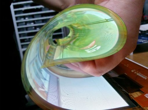
Thanks to silver nanowires, the manufacturing of big curved or really flexible screens ins no longer a target but a concrete possibility.
The reality represented by silver nanowires is commercially available, with various producers that already propose plastic substrates with integrated nanowires, to the extent that, besides “impressive” products like the 42” mentioned at the beginning, already this year is planned the release on the market of toushscreens based on this innovative technology. Another important phenomenon is worth highlighting: the identification of a technology that replaces another one, drastically reducing costs and improving performances, often paves the way to new opportunities for engineers, designers and, in this specific case, the manufacturing of big curved or really flexible screens is no longer a target but a concrete possibility, to the extent that sector analysts foresee a real metamorphosis for touchscreens , with proposals to the maret that were previously unaffordable due to costs. In other words, the availability of high-end transparent conductive materials will lead smartphones, tablets, ultrabooks and other existing devices to be lighter, subtler and faster in their interaction with users.
Not only displays but also sensors
According to what reported until now, it might seem that silver nanowires are only applicable in the production of innovative screens, large and flexible too, with excellent prospects. There is however another ambit in which the researches in course are providing excellent results, i.e. sensors. The researchers of the North Carolina State University have used silver nanowires to develop wearable multitasking sensors able to measure force, pressure and biological signals such as the heartbeat, for applications in biomedical, military and sports field, extending the experimentations to robot systems, too, with a technology that is based on the electrical effects induced by a physical deformation. The developed sensors, deformable and applicable on curvilinear surfaces such as the human skin, can be used to support the development of prostheses able to respond to the movements of a person by activating the opportune feedbacks, to implement robot systems able to perceive the surrounding environment or also, once integrated into a garment, to trace the movement of a person or to monitor his physical conditions. The base is anyway represented by elastic conductors implemented starting from silver nanowires. More in detail, they have conceived a double-layer structure, with two of these conductors separated by an insulating material; in this phase, the two layers can store electric charges, precisely as it happens in the equivalent electrical condenser component, which is characterized by a parameter called capacity. The difference from the condensers of electrotechnics, in this case, is given by the fact that physical stresses of various nature, like pressure, simple touch, stretching and twisting modify the capacity of the element, which is measured by the sensor. In a very significant experiment, they monitored the motions of a human thumb, with results that let us envisage applicative prospects in the control of robots and of prostheses, too. More impressive results have been attained in the monitoring of a knee of a person while walking, running and jumping. It is worth highlighting that the deformations occurring with these movements are particularly wide and significant, and therefore they would have caused the breakage or anyway the malfunction of several sensor typologies, but not of those based on silver nanowires, deformable up to 150% of their original length without losing functionality. Further example, the development of an array of sensors able to map the pressure distribution on a surface, useful performance for robotic applications. Finally, the sensors of the researchers of the North Carolina University show a very fast response time, equal to 40 milliseconds, permitting to monitor parameters essentially in real time.


